The packages are classified on the basis of their mounting position on a circuit board into two types:
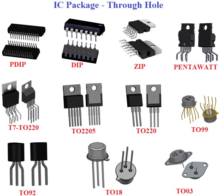
Through-Hole Mount Packages
They are designed during a means that the lead pins are stuck through one facet of the board and smoldered on the opposite. They're larger in size as compared to the opposite kind. These are majorly utilized in equipment to catch up on the board area and price limitations. Twin inline packages are one in every of the samples of through-hole mount packages.
To add on to it classification, Through-hole mount packages are available in ceramic and plastic sorts.
 These square measure the foremost considerably used IC packages is Dual Inline Packages (DIP). similar to in 28-pin ATmega328, the pins square measure placed in parallel to every alternative extending sheer and arranged out on a black plastic housing that is rectangular in form. The pins square measure spaced at 0.1 inches. Further, the package varies in size because of the distinction within the variety of pins in numerous packages. The amount ranges from four to sixty four. These pins square measure placed during a manner that they'll be adjusted on to the middle of a bread board while not short-circuiting one another or maybe get smoldered into PCBs.
There area unit many sorts of DIP Packages, Plastic Dual In-Line Package (PDIP) and Modeled Dual In-Line Package (MDIP) area unit the few common varieties. Further, it may be classified as:
- Standard - this can be the foremost common packaging. The pins area unit spaced 0.1” apart.
- Skinny - during this packaging, the area between the terminal rows is 7.62mm.
- Shrink - kind of like the quality ones however the lead pitch is 1.778 mm. High pin density packaging is used when smaller in size.
- Zig-Zag in Line Packages (ZIP)- The pins during this reasonably a package area unit inserted sheer to the circuit card. This kind of packaging was temporary and was principally employed in dynamic RAM chips.
- Pin Grid Array (PGA)- within the lead pitch is a pair of 2.54 millimetre and therefore the body is formed out of ceramics. The pins area unit organized vertically from the body and may be placed on a grid. This one sometimes suits a multi-pin packaging.
Surface Mount Packaging
Surface mount packaging follows the technology of mounting or putting the elements directly on the computer circuit board surface. Though this method of fabrication helps do things quickly, it conjointly will increase the probabilities of defects. This can be owing to the miniaturization of elements and conjointly as a result of they are mounted extraordinarily on the point of one another. This, in turn, ends up in creating it extraordinarily vital to discover the failure within the entire method. Again, Surface mount packaging conjointly uses ceramic or plastic molding.
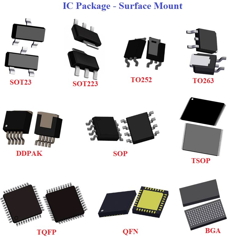
The different forms of surface mount packages that use plastic molds are as following:
- Small define L-leaded package- This kind has gull-wing type leads that lengthen on either direction from the body in associate degree L fashion and may be mounted directly on the board.
- Quad Flat L-leaded Packages (QFP)- These are the same as SOP. However, the sole distinction is that the leads are drawn out in four directions rather than a pair of and are mounted directly on the board. They conjointly escort a sink with intrinsic heat spreader.
- Ball Grid Array (BGA) - These have solder ball arrays on the rear surface of PCBs.
- Fine Pitch Land Grid Array- These have solder land arrays on the rear surface of PCBs.
- Wafer Level Chip Size Package- several Individual chips are created out of a packaged wafer that's cut out.


