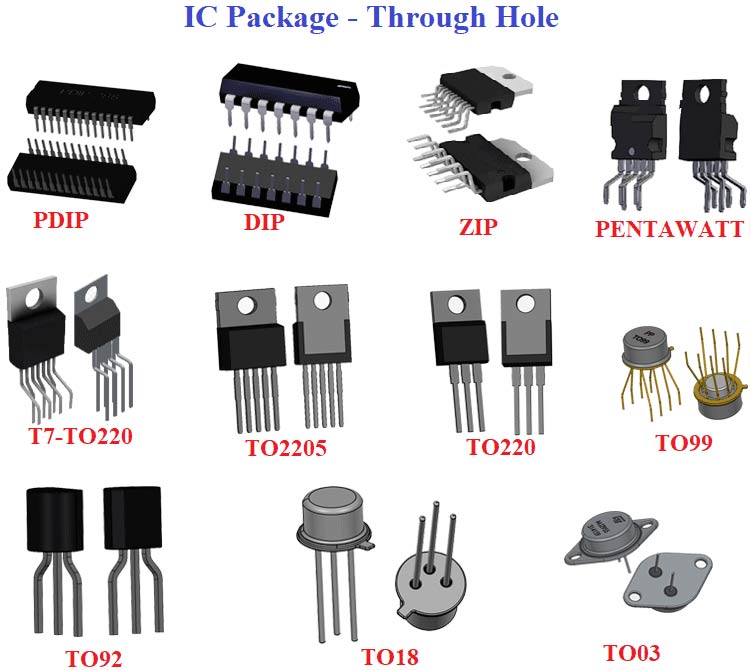
Advanced IC packaging is evolving rapidly, design engineers and engineering managers must keep pace with this significant technology. Before seeking deeper into the packaging technology, it is important to know the fundamental terms that keep coming in advanced IC packaging.
- 2.5D packaging:
In 2.5D packages, dies are stacked side by side on top of an interposer supported through-silicon vias(TSV) . The base, an interposer, provides connectivity between the chips.The 2.5D packages enable finer lines and spaces which is an upgradation to traditional 2D IC packaging technology

3D packaging:
- Chiplets:

Fan out
Fan-out wafer-level packaging (FOWLP)

Heterogeneous integration
The integration of separately manufactured components into a
higher-level assembly provides enhanced functionality and improved operating
characteristics. It enables semiconductor device manufacturers to combine
functional components from different manufacturing process flows into a single
composite device.

- High bandwidth memory (HBM)

- Interposer
It’s a conduit utilized in multi-chip die or boards to undergo electrical signals during a package. An interposer is an electrical interface routing between one socket to another; it either spreads the signal to a wider pitch or takes the connection to a special socket on the board.

- Redistribution layer (RDL)
Redistribution layers are copper metal connection lines or traces that electrically connect one a part of the package with another. RDLs are created with layers of metal or polymer dielectric materials to stack dies on a package and thus relieve the I/O pitch on large chipsets.
- Through silicon via (TSV)

- https://shraddha-kshirsagar18.medium.com/advanced-ic-packaging-1d0bac47e190
- https://riyakaktikar.blogspot.com/2020/12/advanced-ic-packaging-techniques.html
- https://shahikirti24.medium.com/advanced-ic-packaging-requirements-challenges-and-solutions-20c9605108a6
- https://kumbhareruj2000.medium.com/recent-news-in-advanced-ic-packaging-techniques-da9a91d80c2
- https://semiengineering.com/knowledge_centers/packaging/advanced-packaging/chiplets/
- https://anysilicon.com/choose-silicon-via-tsv-packaging-improved-performance/
- https://www.sciencedirect.com/topics/engineering/interposer